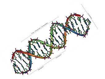
February 21, 2008 (Computerworld) Looking for a way to continually shrink computer chips while still squeezing more transistors onto them, IBM scientists are working on a whole new way to build processors -- using DNA.
For the past year and a half, researchers at IBM have been working on creating a new way to make the patterns used to lay out the transistors and wires that go on a chip. Today, semiconductor manufacturers use optical lithography, which uses light to transfer the pattern. The problem, according to Joe Gordon, senior manager for materials for advanced technology at IBM, is that it's difficult to shrink the pattern using today's techniques.
And since Gordon said 50% of the improvement in processor performance comes from shrinking the pattern, scientists need to come up with a new way to create the patterns.
That's where the DNA strands come into play.
"Right now, the industry road map is [that] we'll get down to 22 nanometer-size features on a chip," said Gordon. "We're looking at ways to go down beyond that. It's very clear it will be difficult to go smaller than that using the optical lithography we know today. Using DNA will help us do that."
Greg Wallraff, a staff scientist at IBM, explained that the researchers are laying single molecules of DNA onto the chip's surface and using them as a template for assembling electronic components, like nanotubes and nanowires. The DNA used by the researchers comes from a virus, he added.
Wallraff said the IBM research team is working with California Institute of Technology scientist Paul Rothemund, who has developed a way to assemble single molecules of DNA into complex structures. Building on that research, the IBM scientists are trying to wrangle the DNA into usable templates.
"People say DNA is the blueprint for life," said Wallraff. "The specific structure of DNA has unique features. It's basically programmable. You can design DNA into unique shapes, with specific attachment sites. Then we pour this DNA solution onto a silicon substrate, and the DNA assembles itself exactly where we want it to on the chip, and then we assemble the components on top of that."
The attachment sites on DNA, which is where the nanowires and transistors would attach on the template, can be made much closer together than with traditional pattern manufacturing techniques. With DNA, the attachment sites are 4nm to 6nm apart. Normally, they're about 45nm apart.
"Think of it as tiling a floor. These DNA pieces are like tiles," explained Gordon. "Each tile has some array of electronic components. Those tiles are placed on a chip in a larger array so there are thousands or millions on a chip. The second step, which we don't know how to do yet, would be to wire them all together. We've got sizes well below conventional lithography."
Once the nanotubes and wires are laid onto the template, the DNA would be extracted. Wallraff said millions of the DNA templates would be needed for a single chip.
Gordon noted that the research team is far from figuring out the whole process needed to make the DNA model work. "We don't have a good picture of exactly how you would do everything," he said. "How do we make the tiles stick together in the right places? Can we get the nanowires to attach to the tiles in the right places? Can we wire them up?"
Wallraff said the next steps will be connect all the tiles together and check the defect levels during assembly.
Actually using this pattern technique is probably 10 to 20 years away, he noted.
IBM scientists look to DNA to build future chips - ComputerWorld, 22.02.2008
